You can also get Class XII Practicals on Biology, Physics, and Physical Education.
Aim : To draw I-V characteristics graph of p-n junction diode in forward biasing and to find state and dynamic resistance.
Apparatus : A p-n junction (semi conductor) diode, a 3 volt battery, a 50 volt battery, a high resistance rheostat, one 0-3 volt voltmeter, one 0-50 volt voltmeter, one 0-100 mA ammeter, a 0-100 uA ammeter, one way key, connecting wires & sand paper.
Theory :
When the p section of the diode is connected to positive terminal and of a battery and n section is connected to negative terminal of the battery then junction is said to be forward bias with an increase in bias voltage the forward current increases slowly in the beginning and then rapidly. At about 0.7 V for SI diode (0.1 V for Ge), the current increase suddenly. The value of forward bias voltage, at which the forward current increases rapidly, is called cut in voltage or threshold voltage.
Procedure
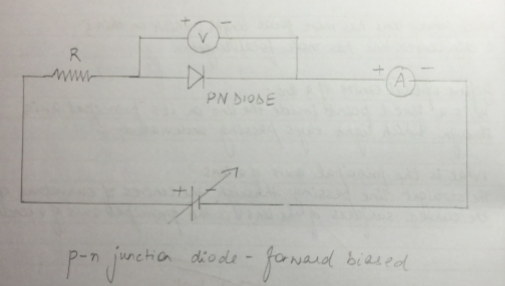
- Make circuit as shown in the circuit diagram.
- Make all the connection neat and tight.
- Note at least count and zero error of voltmeter (V) and milliammeter (mA)
- Bring moving contact of the potential divider (rheostat) near the negative end. Insert the key K. Voltmeter V and milliammeter mA will give zero reading.
- Move the contact a little towards the positive end to apply a forward bias voltage (vF) of 0.1 V current remains zero.
- Increase the forward bias voltage up to 0.3 V for Ge diode.
- Current remains zero ( it is due to junction potential barrier of 0.3 V)
- Increase VF to 0.4 V Milli ammeter records a small current.
- Increase Vf in steps to 0.2 V and note the corresponding current. Current increase first slowly and then rapidly till Vf becomes 0.7 V.
- Make VE = 0.72 V. The current increases suddenly. This represents “ forward breakdown” stage.
- If the VF increases beyond the “ forward breakdown” stage the forward current doesn’t change much. Now take out the key at once.
- Record your observation.
Result
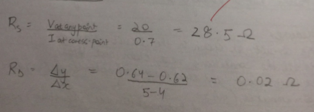
This junction resistance for forward bias :
Resistance (static ) = 28.5 ohm.
Dynamic resistance = 0.02 ohm.
Precaution
- All connection should be neat and tight.
- Key should be used in circuit and opened when not in use.
- Forward bias voltage beyond breakdown shouldn’t be applied.
Sources of error
The junction diode applied may be faulty.
Circuit diagram
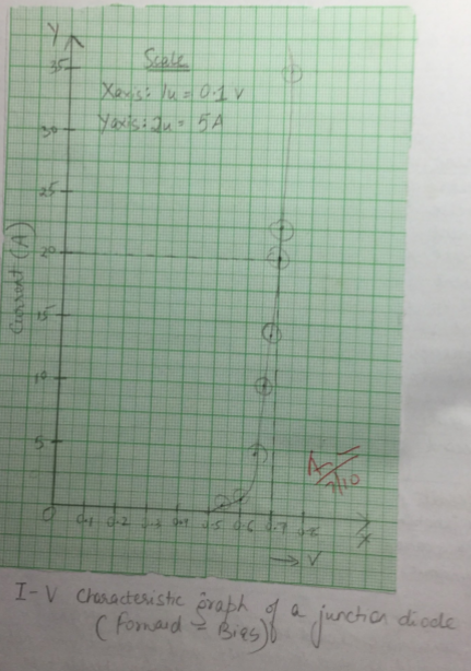
Observation Table
| S No | Potential diff across diode (v) | Current (A) |
| 1 | 0.1 | 0 |
| 2 | 0.2 | 0 |
| 3 | 0.3 | 0 |
| 4 | 0.4 | 0 |
| 5 | 0.5 | 0 |
| 6 | 0.54 | 1 |
| 7 | 0.6 | 2 |
| 8 | 0.62 | 4 |
| 9 | 0.64 | 5 |
| 10 | 0.66 | 10 |
| 11 | 0.68 | 13 |
| 12 | 0.7 | 20 |
| 13 | 0.7 | 25 |
| 14 | 0.72 | 30 |
| 15 | 0.72 | 35 |
Calculation
Viva question
What is a function ?
It is a common surface of n type and p type semiconductor.
What is junction potential barrier ?
The potential difference between junction ends of the two types of semi conductor is called junction potential barrier.
What are the two types of biasing ?
1 forward biasing 2 Reverse biasing
Why is a forward bias so called ? How does it affect junction resistance ?
Forward bias so called because it makes free charge carrier to move forward towards junction . It increases the junction resistance (make less).
You can also get Class XII Practicals on Biology, Physics, and Physical Education.
Very good talentful. Give characteristics curve of Denver diode.
Where is iv character in reverse bias
Mobile
8380850017
Hy super
you have placed v along X axis and I along Y axis.So it is V-I graph not I-V.
Right
current should be in milliamperes not amperes.
It is very helpful us to thanks 😊😊
Really I dont think so
There should be correction in caluclation of static resistance… it should be 0.7/20 instead of 20/0.7 ohm
Why is there an arrow over the battery symbol in the circuit diagram?
It represents variable battery ie its current can be increased or decreased.